- 您现在的位置:买卖IC网 > Sheet目录1917 > DSPIC30F3013-20I/ML (Microchip Technology)IC DSPIC MCU/DSP 24K 44QFN
dsPIC30F2011/2012/3012/3013
DS70139G-page 16
2010 Microchip Technology Inc.
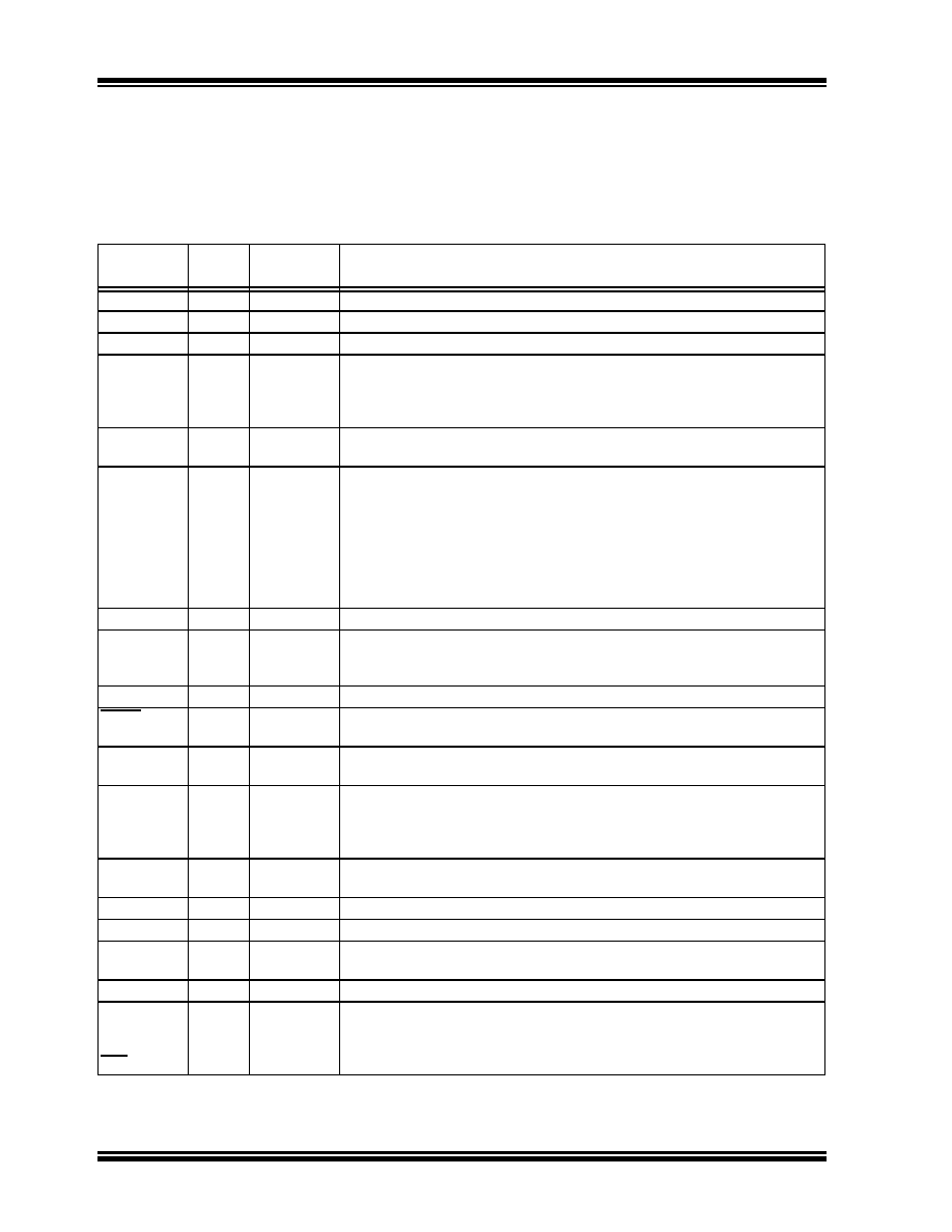
Table 1-1 provides a brief description of device I/O
pinouts and the functions that may be multiplexed to a
port pin. Multiple functions may exist on one port pin.
When multiplexing occurs, the peripheral module’s
functional requirements may force an override of the
data direction of the port pin.
TABLE 1-1:
PINOUT I/O DESCRIPTIONS
Pin Name
Pin
Type
Buffer
Type
Description
AN0 - AN9
I
Analog
Analog input channels.
AVDD
P
Positive supply for analog module. This pin must be connected at all times.
AVSS
P
Ground reference for analog module. This pin must be connected at all times.
CLKI
CLKO
I
O
ST/CMOS
—
External clock source input. Always associated with OSC1 pin function.
Oscillator crystal output. Connects to crystal or resonator in Crystal Oscillator
mode. Optionally functions as CLKO in RC and EC modes. Always associated
with OSC2 pin function.
CN0 - CN7
I
ST
Input change notification inputs.
Can be software programmed for internal weak pull-ups on all inputs.
EMUD
EMUC
EMUD1
EMUC1
EMUD2
EMUC2
EMUD3
EMUC3
I/O
ST
ICD Primary Communication Channel data input/output pin.
ICD Primary Communication Channel clock input/output pin.
ICD Secondary Communication Channel data input/output pin.
ICD Secondary Communication Channel clock input/output pin.
ICD Tertiary Communication Channel data input/output pin.
ICD Tertiary Communication Channel clock input/output pin.
ICD Quaternary Communication Channel data input/output pin.
ICD Quaternary Communication Channel clock input/output pin.
IC1 - IC2
I
ST
Capture inputs 1 through 2.
INT0
INT1
INT2
I
ST
External interrupt 0.
External interrupt 1.
External interrupt 2.
LVDIN
I
Analog
Low-Voltage Detect Reference Voltage Input pin.
MCLR
I/P
ST
Master Clear (Reset) input or programming voltage input. This pin is an
active-low Reset to the device.
OC1-OC2
OCFA
O
I
—
ST
Compare outputs 1 through 2.
Compare Fault A input.
OSC1
OSC2
I
I/O
ST/CMOS
—
Oscillator crystal input. ST buffer when configured in RC mode; CMOS
otherwise.
Oscillator crystal output. Connects to crystal or resonator in Crystal Oscillator
mode. Optionally functions as CLKO in RC and EC modes.
PGD
PGC
I/O
I
ST
In-Circuit Serial Programming data input/output pin.
In-Circuit Serial Programming clock input pin.
RB0 - RB9
I/O
ST
PORTB is a bidirectional I/O port.
RC13 - RC15
I/O
ST
PORTC is a bidirectional I/O port.
RD0,
RD8-RD9
I/O
ST
PORTD is a bidirectional I/O port.
RF2 - RF5
I/O
ST
PORTF is a bidirectional I/O port.
SCK1
SDI1
SDO1
SS1
I/O
I
O
I
ST
—
ST
Synchronous serial clock input/output for SPI1.
SPI1 Data In.
SPI1 Data Out.
SPI1 Slave Synchronization.
Legend: CMOS =
CMOS compatible input or output
Analog =
Analog input
ST
=
Schmitt Trigger input with CMOS levels
O
=
Output
I
=
Input
P
=
Power
发布紧急采购,3分钟左右您将得到回复。
相关PDF资料
DSPIC30F4011-30I/ML
IC DSPIC MCU/DSP 48K 44QFN
DSPIC30F4013-30I/ML
IC DSPIC MCU/DSP 48K 44QFN
DSPIC30F5013-30I/PT
IC DSPIC MCU/DSP 66K 80TQFP
DSPIC30F5015-30I/PT
IC DSPIC MCU/DSP 66K 64TQFP
DSPIC30F6010-20E/PF
IC DSPIC MCU/DSP 144K 80TQFP
DSPIC30F6010A-30I/PF
IC DSPIC MCU/DSP 144K 80TQFP
DSPIC30F6013A-30I/PF
IC DSPIC MCU/DSP 132K 80TQFP
DSPIC30F6014-30I/PF
IC DSPIC MCU/DSP 144K 80TQFP
相关代理商/技术参数
dsPIC30F3013-20I/SO
功能描述:数字信号处理器和控制器 - DSP, DSC 28LD 20MIPS 24 KB RoHS:否 制造商:Microchip Technology 核心:dsPIC 数据总线宽度:16 bit 程序存储器大小:16 KB 数据 RAM 大小:2 KB 最大时钟频率:40 MHz 可编程输入/输出端数量:35 定时器数量:3 设备每秒兆指令数:50 MIPs 工作电源电压:3.3 V 最大工作温度:+ 85 C 封装 / 箱体:TQFP-44 安装风格:SMD/SMT
dsPIC30F3013-20I/SP
功能描述:数字信号处理器和控制器 - DSP, DSC 28LD 20MIPS 24 KB RoHS:否 制造商:Microchip Technology 核心:dsPIC 数据总线宽度:16 bit 程序存储器大小:16 KB 数据 RAM 大小:2 KB 最大时钟频率:40 MHz 可编程输入/输出端数量:35 定时器数量:3 设备每秒兆指令数:50 MIPs 工作电源电压:3.3 V 最大工作温度:+ 85 C 封装 / 箱体:TQFP-44 安装风格:SMD/SMT
DSPIC30F3013-30I/ML
功能描述:数字信号处理器和控制器 - DSP, DSC Sensor RoHS:否 制造商:Microchip Technology 核心:dsPIC 数据总线宽度:16 bit 程序存储器大小:16 KB 数据 RAM 大小:2 KB 最大时钟频率:40 MHz 可编程输入/输出端数量:35 定时器数量:3 设备每秒兆指令数:50 MIPs 工作电源电压:3.3 V 最大工作温度:+ 85 C 封装 / 箱体:TQFP-44 安装风格:SMD/SMT
DSPIC30F3013-30I/SO
功能描述:数字信号处理器和控制器 - DSP, DSC Sensor RoHS:否 制造商:Microchip Technology 核心:dsPIC 数据总线宽度:16 bit 程序存储器大小:16 KB 数据 RAM 大小:2 KB 最大时钟频率:40 MHz 可编程输入/输出端数量:35 定时器数量:3 设备每秒兆指令数:50 MIPs 工作电源电压:3.3 V 最大工作温度:+ 85 C 封装 / 箱体:TQFP-44 安装风格:SMD/SMT
DSPIC30F3013-30I/SO
制造商:Microchip Technology Inc 功能描述:IC DSC 16BIT 24KB 40MHZ 5.5V SOIC-28
DSPIC30F3013-30I/SP
功能描述:数字信号处理器和控制器 - DSP, DSC Sensor RoHS:否 制造商:Microchip Technology 核心:dsPIC 数据总线宽度:16 bit 程序存储器大小:16 KB 数据 RAM 大小:2 KB 最大时钟频率:40 MHz 可编程输入/输出端数量:35 定时器数量:3 设备每秒兆指令数:50 MIPs 工作电源电压:3.3 V 最大工作温度:+ 85 C 封装 / 箱体:TQFP-44 安装风格:SMD/SMT
DSPIC30F3013-30I/SP
制造商:Microchip Technology Inc 功能描述:16-Bit Digital Signal Controller
dsPIC30F3013T-20E/ML
功能描述:数字信号处理器和控制器 - DSP, DSC 44LD 20MIPS 24 KB RoHS:否 制造商:Microchip Technology 核心:dsPIC 数据总线宽度:16 bit 程序存储器大小:16 KB 数据 RAM 大小:2 KB 最大时钟频率:40 MHz 可编程输入/输出端数量:35 定时器数量:3 设备每秒兆指令数:50 MIPs 工作电源电压:3.3 V 最大工作温度:+ 85 C 封装 / 箱体:TQFP-44 安装风格:SMD/SMT